A Primer on Cold Boot Attacks Against Embedded Systems
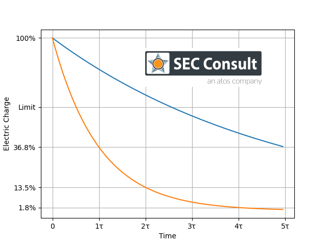
Imagine looking at a picture and then closing your eyes. Immediately, the memory of the picture begins to fade, and you will not be able to reproduce it shortly thereafter. If you are allowed to look at it from time to time again, your memory will be constantly refreshed. Does this behavior mean computer memory does not need to be protected? Can we rely on the data disappearing immediately if the memory loses its power source? As it turns out, it is not that simple when considering the physics involved. The disappearance does not happen immediately – it takes some (very short) time. And because of the temperature-dependent time constant of energy loss in memory cells, this duration correlates with temperature. The diagram below illustrates the correlation between time, data loss and temperature. The blue line shows the charge loss in a memory cell with low temperature, whereas the orange line shows a memory cell with high temperature. It is easy to observe - assuming the data remains readable above the limit illustrated below - that the remaining time to retrieve the data from a cooler cell is a multiple in comparison to the other one.
Therefore, if the memory chip is significantly cooled down, it takes much longer for the data to disappear. If the computer is re-booted after cooling down the memory, previous data can be retrieved. Hence the name cold boot attacks.
Our goal is to use cold boot attacks against embedded systems. In the following, we show how first steps can be taken to achieve this goal. The work presented for basic cold boot attacks uses the Python based LiteX to create a SoC including a Risc V core running on an FPGA development board to interface with the memory of the embedded system. But first, let's get started with some fundamentals.
Cold Boot Attacks
Cold boot attacks have been known in the industry for some years, starting in 2008 with a paper published by Princeton University Lest We Remember: Cold Boot Attacks on Encryption Keys. Targeting personal computers, they exploited physics and the way the memory works in modern computers to recover encryption keys from the systems and to break hard disk encryption. As the researchers already noted, such attacks are quite difficult to prevent. Therefore, since then, manufacturers have tried to develop solutions to prevent these attacks or make them harder to conduct. And researchers have discovered new ways to exploit them. One of the most recent publications is The Chilling Reality of Cold Boot Attacks, where researchers from F-Secure circumvented the countermeasure of overwriting memory after power is restored in order to execute a cold boot attack. Extensive information on this topic is available online.
A typical cold boot attack is executed on a running but locked computer in the following way: While the computer is still running, it is opened, and the DRAM modules are cooled down with cooling spray to extend the time they retain their contents. After that, a hard shutdown is executed (pulling the power plug) and the system is booted from a prepared media containing memory dumping tools with a minimal memory footprint to extract the preserved memory content. Alternatively, the memory modules can be removed from the computer and transferred to another system to be dumped.
Embedded Systems
Over the last decades, embedded systems have taken over the world. Everything has become smart and often communicates with other devices, resembling the Internet of Things. As we use more and more of these devices, attacks seen on personal computers (and often got mitigated or contained to some extent) are being transferred to the domain of embedded systems. However, as these systems are very different and resemble a highly heterogeneous landscape, their unique designs and limitations pose special challenges to hardware attacks.
In contrast to highly standardized consumer computers, embedded systems come in many different shapes and performance levels, using hardware and software tailored for their task. Additionally, they are designed for size and durability, leading to the use of non-removable memory elements and different, optimized DRAM interfaces. The software running on the devices is barely compatible and the available external boot options are restricted, making the use of a single external boot media unfeasible. All this means that developing a single solution, which can be used by multiple systems is very difficult and requires a lot of effort in the world of embedded systems.
To work on this topic, some low-level knowledge about DRAM, its interconnection within the architecture and about the fundamentals of embedded systems is required. In the next section, we'll take a deep dive into this matter.
From Theory to Practical Experience
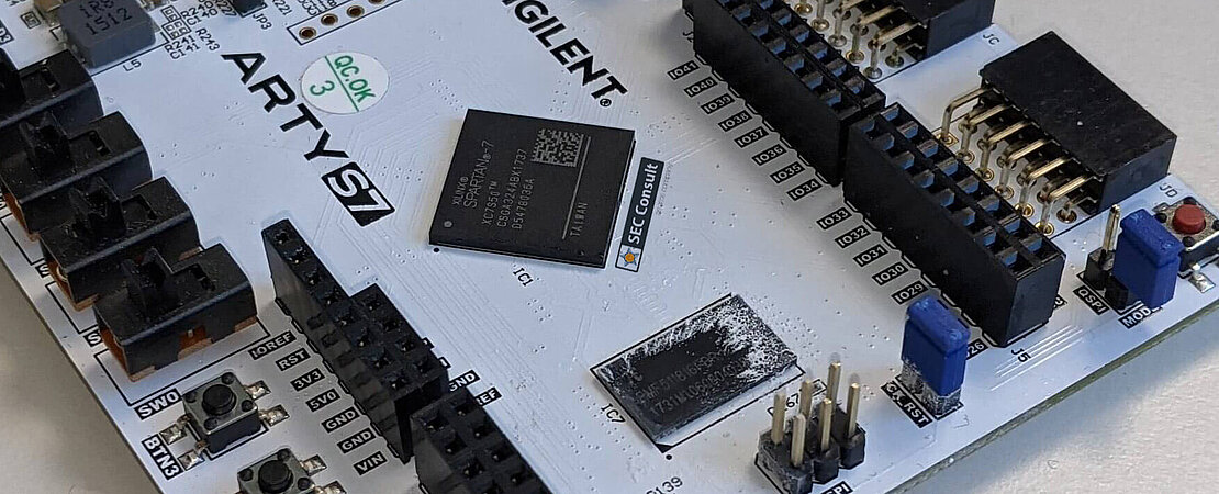
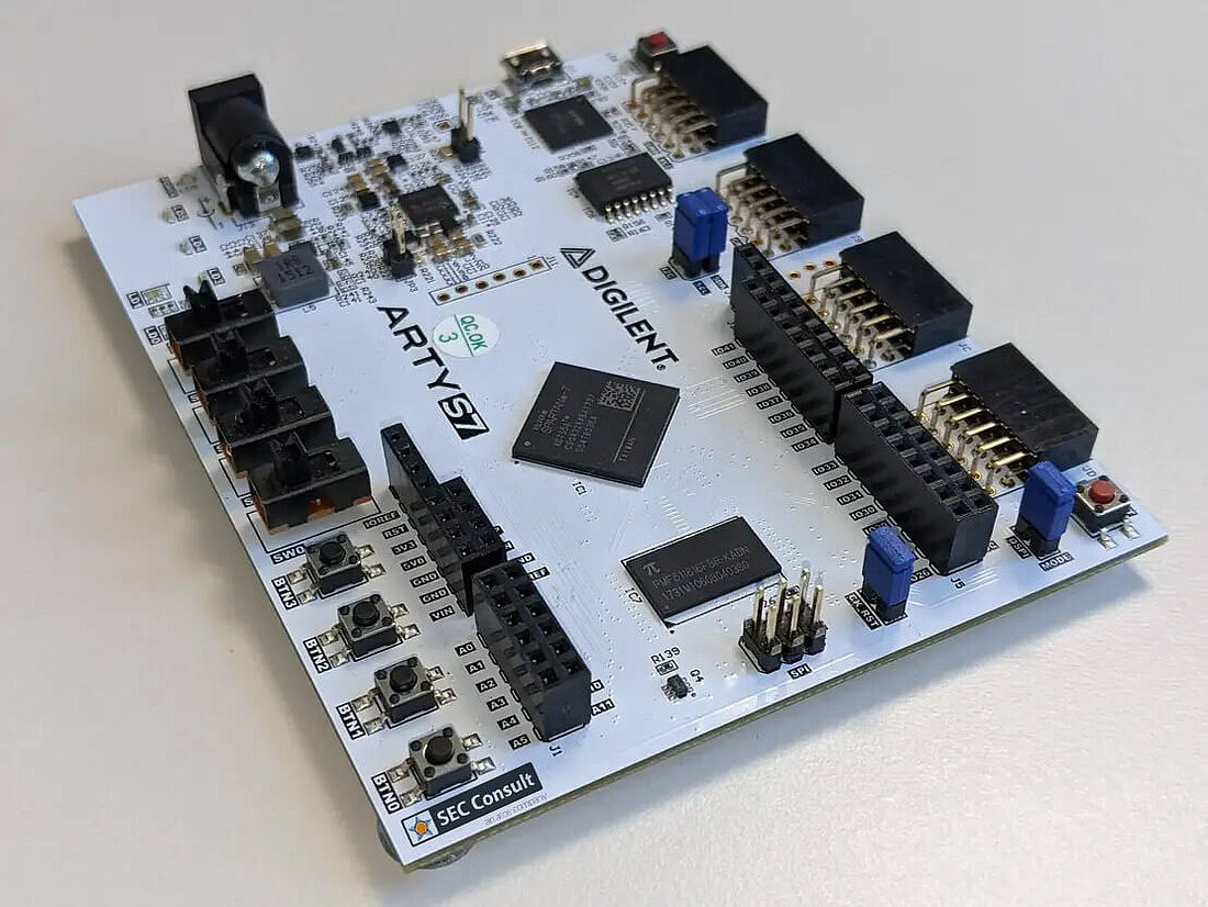
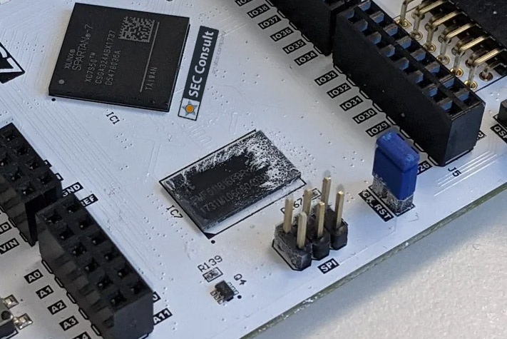
An FPGA design was used to achieve some flexibility and support re-usability as well as extensibility. FPGAs work like computer chips, but you can program them to be whatever you can code. For this, a Hardware Description Language (HDL) is used. The first step towards being able to perform cold boot attacks on numerous devices is to start simple and create a solid basis. The used demonstration and development platform is an Arty S7-50 (REV E) containing a Xilinx Spartan-7 FPGA and 256MB DDR3L memory. Extensive information about this board can be found online. The DRAM chip itself can be identified as Piecemaker PMF511816FBR (datasheet).
First Steps with LiteX - Does Python fit Hardware Development?
The LiteX project will be used as software base. It is an open source SoC builder for easy creation of SoCs with various components and was also introduced in Bunnie's blog a few years ago. One part of the LiteX project is the LiteDRAM module, which is the particular reason for choosing this project. It offers a wide selection on physical DRAM interfaces, supporting DDR, LPDDR, DDR2, DDR3, and DDR4 on different platforms with a (comparatively) easy way to create additional ones. The centrepiece of the platform is a Risc V core, namely the VexRiscv implementation for FPGAs.
The project uses Python to configure and stitch everything together. First, the design is created in Python and then translated into HDL by LiteX. It can be used by existing open-source or vendor toolchains to generate the FPGA bitstream. Creating hardware designs in Python code may feel unusual for hardware engineers used to HDL code, but it turns out to offer some nice advantages for fast creation and modification of SoC designs at a high abstraction level.
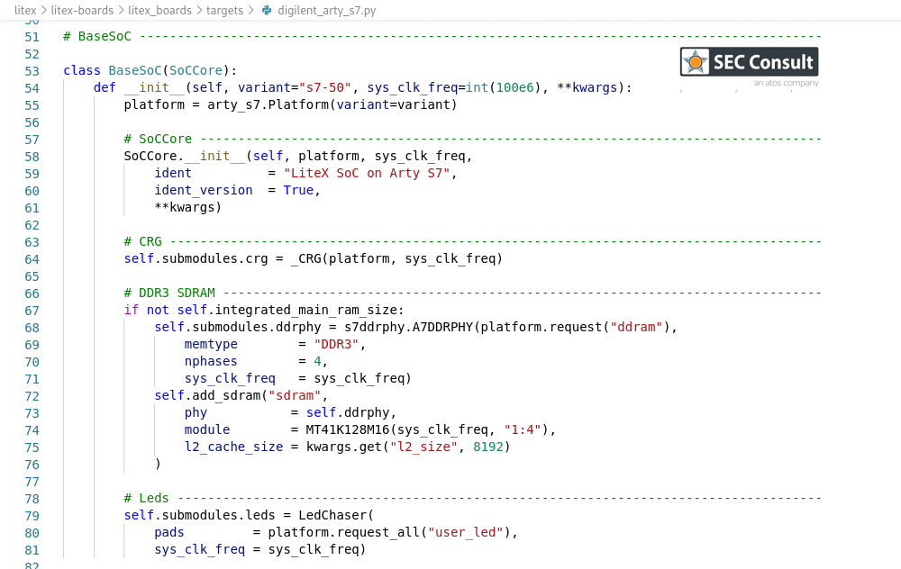
Now it's time to get our hands dirty. The target configuration can be found in litex-boards/litex_boards/targets/. As the board is already supported by LiteX, a target is already available.
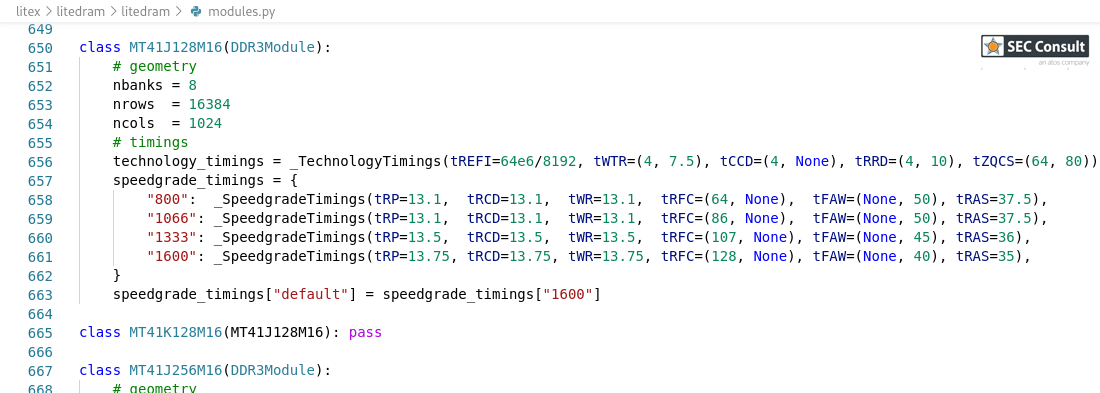
The configuration shows that a Micron MT41K128M16 DRAM implementation is configured. This does not match the chip that we have identified above. However, after consulting the datasheet, it seems that the chips are compatible and have similar timing requirements. Therefore, we can use the same implementation. The DRAM implementation for the configured module is shown below. New modules can also easily be added to this file with LiteDRAM.
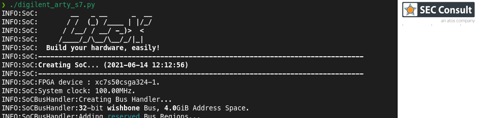
The build process is started by executing the platform configuration script in litex-boards/litex_boards/platforms/ for our board. Using the command line options, multiple parameters can be set (including the UART speed to retrieve data faster).
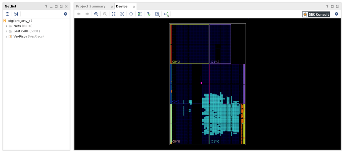
The script now creates a project together with a Verilog file of the configured SoC. In addition, a TCL configuration file is created for use with the Xilinx Vivado toolchain. After importing the project in Vivado, the FPGA bitstream can be generated. An FPGA consists of many cells - little building blocks that are used and connected to provide the programmed functionality. The screenshot below shows a visual depiction of the design's resource usage on the FPGA.
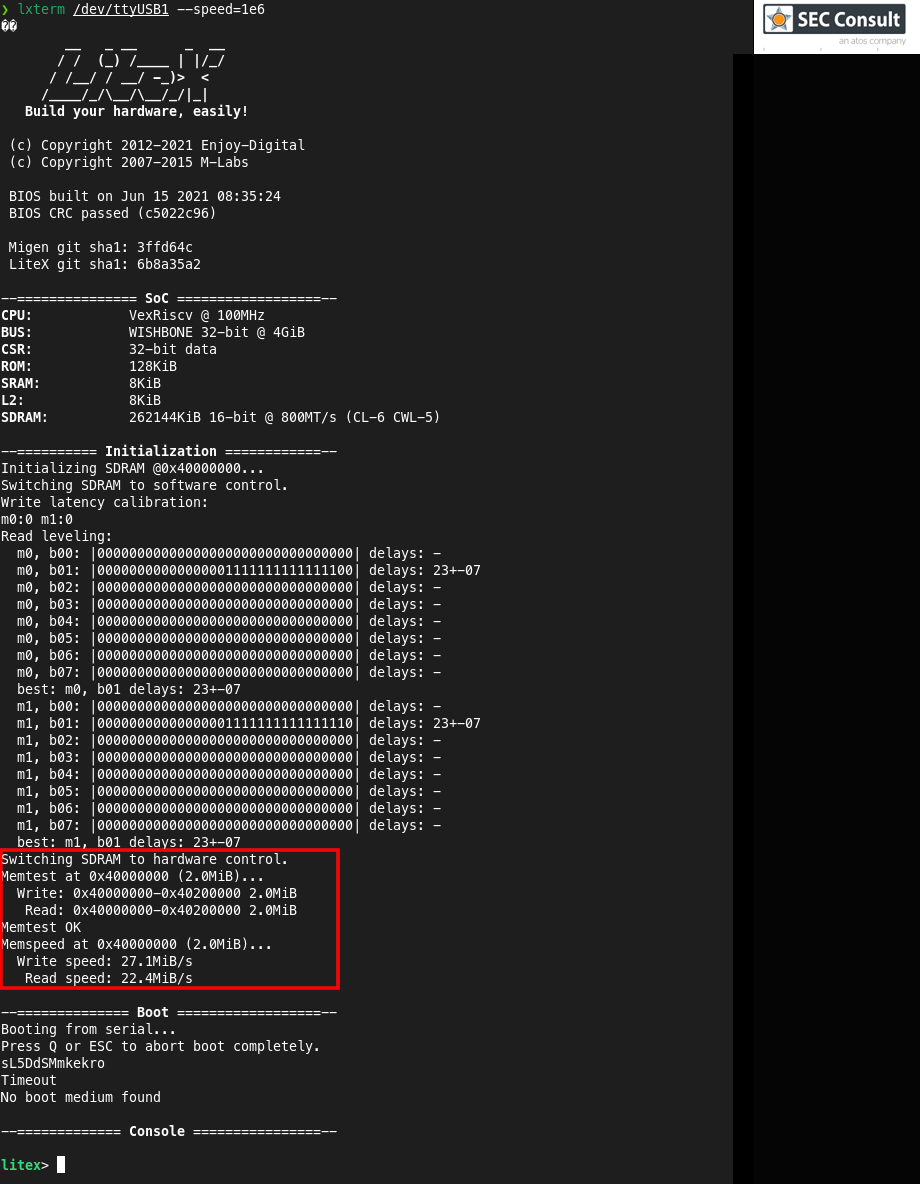
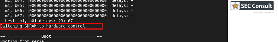
The design already includes a small bootloader (called LiteX BIOS), which is accessible via the UART USB bridge. After transferring the bitstream to the Arty board and starting to listen on the UART interface, the first boot of the system can be observed.
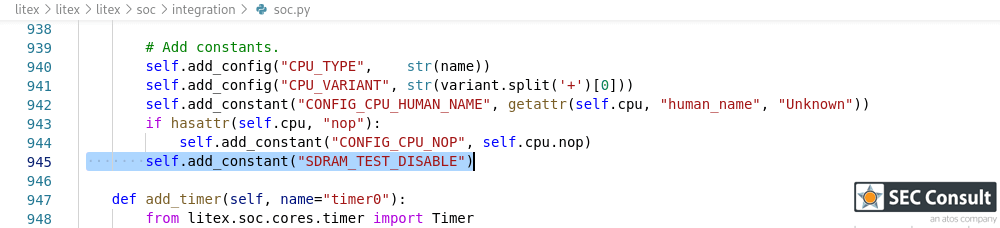
However, it seems that a memory test is configured, which overwrites 2 megabytes of our precious memory that we want to recover. But due to LiteX, reconfiguration is easy. It is Python, after all. Adding the compile flag shown below, it is enough to disable the memory test and to stop this behavior.
After rebuilding the LiteX and Vivado project and reprogramming the device, the on-boot memory test disappeared.
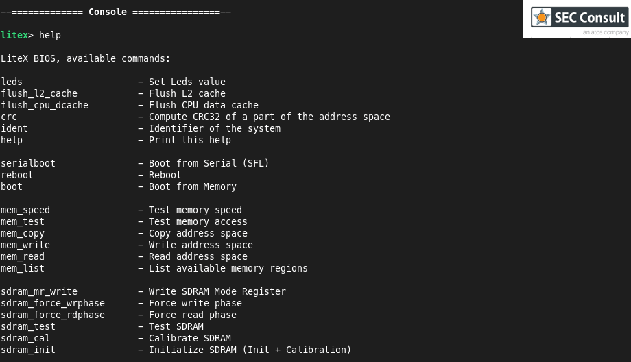
The LiteX BIOS provides some valuable memory access functions. They come in handy to proof the point of a cold boot attack.
Cold Boot Attack Example
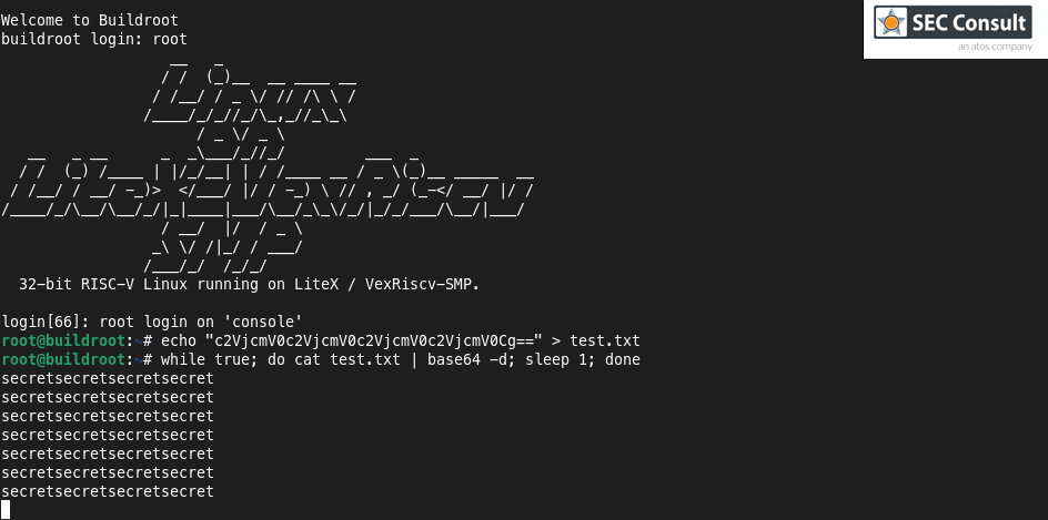
For the attack itself, another LiteX project can be used, Linux on LiteX. This project provides a guide and sources for running Linux on a SoC created with LiteX and is used as a victim application to demonstrate the attack. In addition to the build instructions, precompiled images are available. The system images can be loaded via the serial port. Due to the limited serial port speed, this takes several minutes. After Linux has been successfully started, we can login to a root shell and create a file containing a Base64 encoded secret. Using the shell, this secret is now processed on the system (it is decoded and printed every second). Note that the secret is never stored on disk but only processed during execution in memory.
Now, as the victim's secret is set, it's time to carry out the attack. This is started by cooling down the DRAM chip to extend the data lifetime of the memory.
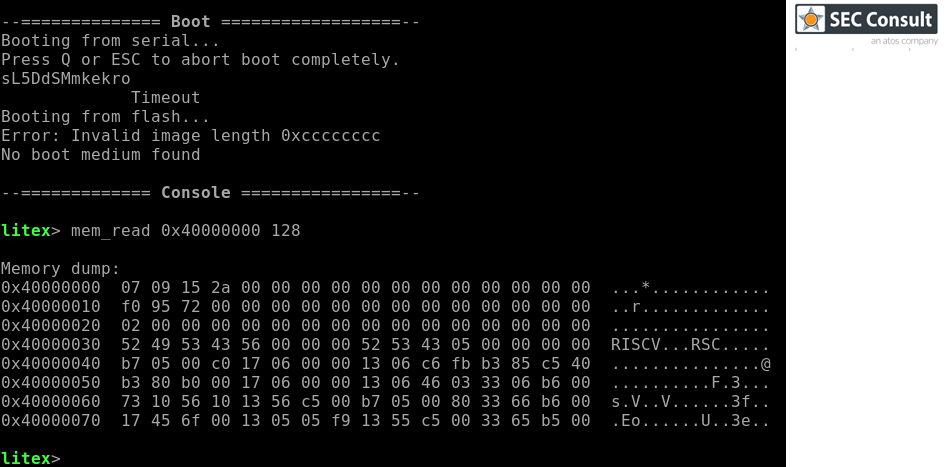
After that, we can power cycle the board and connect and reprogram the system. This time we boot to the LiteX BIOS already shown above. Here, the available memory commands can be used to read its content. The boot log from above shows that the memory is mapped to address 0x40000000. Therefore, we start dumping the data from this address.
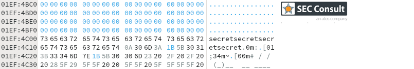
The size of the whole memory is 256MB, hence we need to dump 0x10000000 bytes to get the whole memory content. To process the memory dump efficiently, the output of the dump must be logged to a file. For simplicity, this text can also be reverted to a binary file using the xxd utility. The dump reveals the secret in two different places when being searched for.
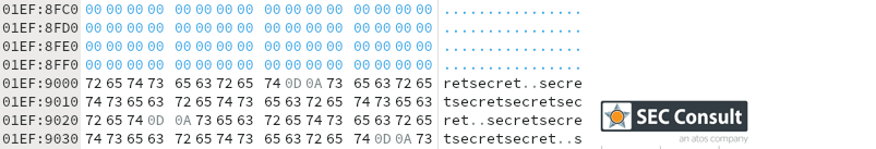
The attack succeeded, now we have successfully recovered the secret from the memory of the embedded device.
From Practical Experience to Applicability
Apart from some limitations, the basic approach presented in this blog post can already be used on FPGA-based embedded systems. To execute an attack exactly as shown above, we need to be able to reprogram the FPGA on the target device (this should not be possible on properly secured devices). In addition, the FPGA, the DRAM model and physical interface must be supported by LiteX or coded on our own, which requires some knowledge and can involve a considerable amount of work.
The next challenge is to overcome these limitations and to generalize this approach by connecting prepared hardware directly to the memory interface traces and therefore without the need to program the target device. This provides some significant improvements and extends the range of exploitable devices by making the attack applicable to properly secured devices or devices which are based on microcontrollers. However, additional hardware engineering work is required to address the various memory form factors. And since the memory interface is one of the most timing-sensitive buses of a system, there is even more physics that must be considered.
This research was done by Gerhard Hechenberger on behalf of SEC Consult Vulnerability Lab.
SEC Consult is always searching for talented security professionals to work in our team. More information can be found at: https://www.sec-consult.com