Reverse Engineering Architecture And Pinout of Custom Asics

hardware vulnerability

Learn about the process of initial reverse engineering the pinout of unknown ASICs by using moderate methods. The two described ICs are good examples out of many industry-solutions and have been chosen to demonstrate how design decisions from vendors are made. The exploited potential leak of the supply-chain can be leveraged by a hardware reverse engineer to extract internal information about such systems.

By Exploiting potential Supply-Chain Leaks

The following article describes some straight-forward hardware reverse engineering methods. It covers the process of initial reverse engineering the pinout of unknown ASICs by using moderate methods. The two described ICs are good examples out of many industry-solutions and have been chosen to demonstrate how design decisions from vendors are made. The exploited potential leak of the supply-chain can be leveraged by a hardware reverse engineer to extract internal information about such systems.

During this research, conducted in SEC Consult Vulnerability Lab’s dedicated Hardware Security Lab, the widely used Siemens S7-1200 series (with focus on the newest v4 series) was thoroughly investigated. The chip family and more than 60 percent of the pins from the chip of the older series (between v1 and v3.0) were identified. As a novelty, the chip architecture and about 70 percent of the pins of the new series could also be reverse engineered. A precise identification of the used internals allowed us to debug the chip with JTAG and inspect internal registers during run-time. 

Other vendors have similar devices in their portfolio and we think that the same circumstances apply to that products as well. Nevertheless we did not test others in this research.

Over the past, people of the electronic and computer science community demonstrated a lot of creativity regarding their embedded devices.

Firmware hacks and hardware modifications of routers, access points or even oscilloscopes have been presented in forums and blogs on the web ever since. During the necessary reverse engineering processes, a lot of documentation arises as a byproduct. This valuable information can be extremely useful, especially when working with expensive or rare devices.

Experienced reverse engineers with knowledge of hardware and firmware can dissect an un-hardened product with known parts (and available datasheets) without problem. The biggest enemy of such endeavors are undocumented black-box ASICs, which are impossible to find on the Internet – and if at all, only with unhelpful information. These ASICs rarely turn out as real full custom ASICs but are mostly custom SoCs created with standard-cells. As design re-use saves much development time and can speed-up the tape-out, most vendors, which create such customized solutions, use a basic set of existing modules from their repository. This fact helps to determine a lot of internals within unknown chips!

Additionally, such information could be used to build backdoors into hardware. A popular case of a potential backdoor in hardware was lastly claimed by Bloomberg in October 2018 regarding the Supermicro server boards. However, SEC Consult did not find evidence that there was any backdoor in the reversed hardware in scope of this blog post and we did not look for them either.

Photo of the target device. (c) SEC Consult Vulnerability Lab

Become Acquainted With Your Target 

A textbook example for a publicly completely unknown chip is the SoC inside of the S7-1200 PLC series which is a product from the market leader Siemens. This embedded device is used in many different industrial applications for controlling purposes. Besides the industrial interfaces, this PLC also has an ethernet port and a web-server embedded in its newer firmware versions (3.0 and up).

That we have chosen this specific device was only because of its wide use. The here described circumstances and findings could affect any other vendor of specific ASICS in the same or a similar way. 

Boards on Taobao. Good-to-know: Siemens is written as 西门子 (Xī mén zǐ) in Chinese. (c) SEC Consult Vulnerability Lab

A quick look on the Printed Circuit Board (PCB) of the S7-1212C reveals an Ethernet PHY, a Flash Chip, a RTC, a Quartz and other parts. The used SoC is labeled with its country of origin “JAPAN” and “MB87M2230” as part number, and other identifiers on the chip of unknown meaning. Since this PLC model is too expensive to wreck more than one board just for fun, a more cost-effective way was needed.

Searching on the internet for this SoC does not turn up many results. Less than 100 sites from China are popping up during research and also the e-Bay like shopping site Taobao (淘宝). This finding proved really important, since multiple different devices with the same unknown chip are usually the ideal starting point for successfully reverse engineering.

Help From SHÀNTÓU (汕头) – Assumed Supply Chain Leak #1

The devices from a seller in Shàntóu (a city in China) seem to be some kind of evaluation board. Selling such a board is an indication of a supply-chain leak. The SoC of the Siemens PLC was also located on the devices and that makes it interesting. The boards were labeled with the price of 10¥ (March 2018: ~1.3€), which is very cheap in comparison to the S7-1212C (~260€). After a request for five pieces the seller offered them for 95¥/12€ per piece, which is still cheaper than the original PLC.

Example boards from a Chinese reseller - SEC Consult
Example boards from a Chinese reseller. (c) SEC Consult Vulnerability Lab
Close up of PLCs from Chinese reseller - SEC Consult
Close up of PLCs from Chinese reseller. (c) SEC Consult Vulnerability Lab

A few weeks later, the boards finally arrived in the SEC Consult Hardware Security Lab in Vienna. Some components were missing or were nearly busted off, it looked as if these boards were directly collected from an e-waste site and shipped to us.

At least one of the five boards worked and broadcasted its MAC address with the fingerprint of the actual vendor. That means, that the Ethernet stack works and at least one CPU is alive. This was a first important indication that the board is not a kind of fake electronics. Everyone could solder some random parts on a PCBand sell it online.

Front side of the PCB - SEC Consult
Front side of the PCB. Arrows indicate a communication channel. (c) SEC Consult Vulnerability Lab
Back side of the PCB - SEC Consult Vulnerability Lab
Back side of the PCB. (c) SEC Consult Vulnerability Lab

After a quick identification of the ICs, a search on the web returned the datasheets of the usual electronic parts. All suspected VCC and GND pins of the ASIC, which were determined by simply measuring its voltage, must be collected and used later because one cannot completely rely on the bare voltage levels of the pins.

Naked PCB without parts - SEC Consult
Naked PCB without parts. (c) SEC Consult Vulnerability Lab
QR-Code in Data Matrix format on the PCBs - SEC Consult
QR-Code in Data Matrix format on the PCBs. Information: 1PA5E02508288+SVPDN289375+30P04+7Q06+1Z1 (c) SEC Consult Vulnerability Lab

An experienced reverse engineer will immediately recognize the header in the middle of the PCB backside as possible JTAG-header. This was also the first intention but as we figured out later, this was much harder than expected.

First of all, one board must die! The most destructed device was the source of the first pinout of the MB87M2230. After it was completely freed from the electronic parts on it, the traces can be followed to the other components with a multi-meter. A quick look on both sides revealed the connections between Flash, SDRAM, Ethernet PHY and the clock source. By inspecting the back-side of the PCB a QR-code was spotted. This code is suspected to represent the same kind of a serial string for the boards.

Diagram of ram architecture including flash memory, EEPROM and the power circuit - SEC Consult
Example architecture: Known parts with datasheets are the RAM, Flash Memory, EEPROM and the power circuit. These interfaces of the unknown SoC/ASIC can be determined by following the traces. The power pins can be measured in the circuit but must be verified by additional measurement after removing the chip from the PCB. (c) SEC Consult Vulnerability Lab.

Deductive Reasoning – Passive

The unpopulated board can be used to measure the connections to the known parts and the unknown ASIC. Since the bus interfaces in the most SoCs are predefined function-blocks, the CFI and the RAM interfaces can be determined from the connections to flash memories (NAND/NOR) and RAM parts. By using multiple sources (c.f. different PCBs with the same ASIC of interest), most pins, which are outfitted with these interfaces, can be found easily. The pin count of an interface (e.g. address buses of DRAMs) cannot be completely revealed when the bus width is not fully utilized in any of the investigated PCBs.

JTAG brute-forcing with the SEC Xtractor (a hardware testing tool developed by SEC Consult which was first mentioned in this blogpost). (c) SEC Consult Vulnerability Lab.
JTAG pinout on the board - SEC Consult
JTAG pinout on the board. The resistor which is bound to VCC must be changed to GND in order to activate the interface. Such JTAG ports are usually only mounted on development or evaluation boards. (c) SEC Consult Vulnerability Lab.

Another valuable source to find pin functionality is the ASIC itself. Suspected GND and VCC pins can be measured for connectivity after the initial identification which was described in the last section. The power grid inside of the ASIC is usually connected and these connections can be measured from the outside. Anticipated power pins, which are not directly connected to the power grid but permanently connected via a resistor to VCC or GND on both PCBs, are in many cases unused debug interfaces, pins with specific functions when asserted to logic “1” or logic “0” and reference voltage pins.

Another indication for a “real” power pin is also a ~10nF capacitors around a pin. This is helps to avoid glitches on the power supply.

Probing Methods – Active

One of the hardest challenges on undocumented electronics is the reliable detection of debug-interfaces. To be honest, the PCBs from the dealer on Taobao helped a lot, but it is not always that easy! Usually, there are no boards with debug interfaces that can be found on the internet.

The previously mentioned well-known JTAG header seems to be the ultimate gateway on gaining access to this ASIC. At first glance, it looks like a 20-pin ARM-JTAG-interface but RCLK was missing. This means that adaptive clocking is not needed or not configured, or it is another architecture. Regardless, it could be any other CPU core or a completely custom architecture.

The first tries with the SEC Xtractor, a self-built hardware and software solution to brute-force the interface, failed. Too many pins were excluded (because they are not connected to the ASIC) from this header and just six pins were left. But it would be a pity to give up at this point.

ID Code found - SEC Consult
ID code found!

A very common way to deactivate debug interfaces is to simply gate it behind transistors. This can be done in both directions and prevents accidental stimuli and also unwanted actions from reverse engineers.

One pin from the ASIC, which was close to the other suspected debug pins, was pulled to logic “1” with a resistor. Next to the resistor was another header for a resistor pulling to logic “0”. After removing the resistor from its original position and soldering it to the alternative header, the JTAG port was activated. This kind of deactivating the debug interface is widely used but not very effective when someone really wants to access the ASIC. In general, there are other methodologies like physical anti-fuses to permanently kill JTAG.

After resoldering the resistor, the interface was immediately found by the SEC Xtractor solution. By changing the Xtractor to OpenOCD mode, a Test Access Port was automatically detected. The ID code of the chip was 0x1406c009..

JTAG ID code bit - SEC Consult
JTAG ID code bit partitioning with the set bits for the MB87M2230. It may vary for other vendors. The JEDEC standard “JEP106AV” can also be used for vendor identification. It contains all vendor codes and is constantly updated. Apart from the debug port, the IR (Instruction Register) length was also brute forced and found to be 5, which was also detected by OpenOCD. (c) SEC Consult Vulnerability Lab

To understand why the OpenOCD prints the vendor code 0x004, the part number 0x406c and the version 0x1 it is essential to know how the JTAG ID code is partitioned in general:

This is a wire-bonding example for a transistor. The same technique was used for this IC. In microprocessors or microcontrollers the bonding-wires are usually made of gold or copper. Image from Inductiveload [CC BY-SA 3.0]. Source: https://commons.wikimedia.org/wiki/File:Wirebonding2.svg
Sketch of QFP chip inside - SEC Consult
Source: https://www.fujitsu.com/downloads/MICRO/fma/pdfmcu/packageguide-contents-x1.pdf

There are more advanced methods for active probing, but these are not covered here.

Digging Deeper

After chasing for pin functionality, a more invasive method was used to get some information. The IC was boiled in sulfuric acid and cleaned with nitrogen thinner (don’t try that at home, folks!). The exposed die, which was previously covered by the package, was relatively small (Die:Package – 1:5) in comparison to its housing. That was caused by the chosen wire-bonding technique.

Stitched die-shot of the FUJITSU MB87M2230. (c) SEC Consult Vulnerability Lab

The IC was inspected with a metallurgical con-focal microscope to locate not connected pins and find valuable information like vendor name, internal information and other labels. To be honest, we expected chip-arts like the ASICs of ETH Zurich: http://asic.ethz.ch/cg/all/imagemap.html – Mr.Wolf. They look amazing!

A simple die-shot was stitched together by using multiple images with the lowest zoom:

Chip with the number MB87M2230 - SEC Consult
Part number “MB87M2230” and vendor name FUJITSU. The “A”s beneath the label represent the layers of the die. They can be spotted easily by changing the focus of the microscope to the corresponding layer. The big mirrored “1” indicates pin 1 (it is mirrored because of the microscope). (c) SEC Consult Vulnerability Lab
Picture shows a pad at the highest zoom which is labeled with “NC" - SEC Consult
Pad with “NC” (Not Connected) label. (c) SEC Consult Vulnerability Lab

This can also be used for identification of fake-parts. The orthogonal and sometimes yellow lines are power, ground and clock distribution nets. They are arranged in that shape to minimize clock skew and power glitches. On the edges of the die a lot of rectangular blocks are located. They are called bonding-pads and are the physical connection to the world outside. The structure which is arranged in a grid, is visible especially on the upper right quarter of the die. This is a good indication for a standard-cell ASIC.

Some information was found on the die of the IC. For example the company “FUJITSU” which is at least the designing company of the SoC and the copyright label “©2007″ which is probably the creation year of the design. This confirms the gathered information from the chip ID which was found via the JTAG port. The chip number MB87M2230 can also be found on the metal layer of the IC which is beside the multiple “A”s, used as layer markers, the last part of hidden information on the chip. The chip has six layers, pin 1 is also located in this edge.

Zoom factors. Microscopy is fun! (c) SEC Consult Vulnerability Lab

In this case no “NC” pin was actually bonded. The bonded pads are easy to determine because they have old contact traces from previous wire-bonds. The latter picture shows a pad at the highest zoom which is labeled with “NC”. Chip manufacturers sometimes write more information on the die.  A comparison of the different zoom factors is shown on the following picture:

Fujitsu microprocessor roadmap - SEC Consult
Fujitsu microprocessor roadmap from 2000. Source: https://www.fujitsu.com/global/documents/about/resources/publications/fstj /archives/vol36-1/paper06.pdf
Fujitsu microprocessor roadmap - SEC Consult
Fujitsu microprocessor roadmap from 2012. Source: http://docplayer.net/4207609-Right-sized-solutions-for-embedded-applications.html

Literature and Code Review

A review of various Fujitsu presentations and datasheets revealed that the architecture of the MB87M2230 can be ARM, ARCTangent A4, F²MC or FR / FR-V. The architecture Fujitsu RISC (FR) is based on SPARClite. Two publicly available roadmaps from 1996 to 2013 are shown in the following graph:

Empty NOR flash socket - SEC Consult
Empty NOR flash socket. (c) SEC Consult Vulnerability Lab
NOR flash memory - SEC Consult
NOR flash memory plugged into the adapter shield of the new (red) SEC Xtractor 1.20 solution. (c) SEC Consult Vulnerability Lab

To clarify which processor type resides in the ASIC at hand, the NOR flash memory from the PLC device (S7-1212Cv1) was removed and dumped with the SEC Xtractor solution.

Decompiled pseudocode of the NOR flash memory - SEC Consult
Decompiled pseudocode of the NOR flash memory which is connected to the MB87M2230. (c) SEC Consult Vulnerability Lab

The memory was quickly examined with binwalk. Based on its output the CPU architecture looks like an ARM big endian:

$ binwalk -A dump.bin
DECIMAL       HEXADECIMAL     DESCRIPTION
--------------------------------------------------------------------------------
65576         0x10028         ARMEB instructions, function prologue
67096         0x10618         ARMEB instructions, function prologue
67156         0x10654         ARMEB instructions, function prologue
68236         0x10A8C         ARMEB instructions, function prologue
68448         0x10B60         ARMEB instructions, function prologue
68520         0x10BA8         ARMEB instructions, function prologue
68580         0x10BE4         ARMEB instructions, function prologue
68652         0x10C2C         ARMEB instructions, function prologue
68772         0x10CA4         ARMEB instructions, function prologue
68840         0x10CE8         ARMEB instructions, function prologue
68852         0x10CF4         ARMEB instructions, function prologue
68956         0x10D5C         ARMEB instructions, function prologue
68996         0x10D84         ARMEB instructions, function prologue
69036         0x10DAC         ARMEB instructions, function prologue
69076         0x10DD4         ARMEB instructions, function prologue
69124         0x10E04         ARMEB instructions, function prologue
69164         0x10E2C         ARMEB instructions, function prologue
69204         0x10E54         ARMEB instructions, function prologue
69244         0x10E7C         ARMEB instructions, function prologue
...

At this point, it is clear that an ARM core is used for this ASIC. By looking on the 5-bit long ID code which was brute-forced before, it may be an ARM11xx core when the ID is not customized (which is likely).

By using the ARM big endian architecture for IDA Pro with the previous dump, many functions were found but not all data blocks and further functions were referenced automatically. This process would require a lot of manual work and a lot of time, but ARM big endian seems to be the right architecture.

Image shows available IP cores for the Fujitsu CMOS - SEC Consult
Available IP cores for the Fujitsu CMOS CS81 / CMOS CS86 technology and others are a good example for design re-use. [Source: http://www.fujitsu.com/downloads/MICRO/fme/asic/asic-ip-and-cores-fme-c32-0407.pdf].

Based on many strings, it was easy to recognize that the whole system was built with C++. Furthermore, it was possible to detect modules of the whole SoC in the code where some are obvious and others are hidden.

Next, let’s combine that knowledge with the fact that the original design of this chip was made in 2007 and that the IR length is 5. The circumstance that adaptive clocking is just disabled means that there could be a RTCK pin which cannot be matched easily from that point, but this is not necessary. By referring to the ARM infocenter we can say that there is just one ARM core which would fit into the scheme, the ARM11xx series. One bit less (or because this is customized) can also lead to the assumption that it is the ARM9xx series. The used package (LQFP-208) and the CMOS 180nm process from Fujitsu let also conclude the same because ARM11xx is (or was) not available as IP core referring to a presentation.

Block digram of the MB87M2230 - SEC Consult
Block diagram of the MB87M2230. This architecture is estimated of course. (c) SEC Consult Vulnerability Lab

However, it’s precise enough to identify an ARM processor designed around 2007 as CPU. Similar chips from Fujitsu like the MB87M3550 use an ARM926 core.

The Big Picture

The pinout for the LQFP-208 package was partially reversed but is not published yet to avoid any abuse. An architectural schematic can also be drawn by combining the obvious hardware architecture of the peripherals with the additional information of the dumped firmware:

The BGA chip in the center of the PCB of hardware version 4 - SEC Consult
The BGA chip in the center of the PCB of hardware version 4 is labeled as “Siemens A5E30235063” chip. Source: http://s7detali.narod.ru/.
The quadratic chip in the center of the PCB is a BGA housing - SEC Consult
The quadratic chip in the center is a BGA housing which is labeled with “MB87M2230”. Source: http://s7detali.narod.ru/.

More Electronics - Potential Supply Chain Leak #2

Thanks to a Russian web-site, where a huge collection of Siemens PCB pictures can be found, more versions of the Siemens S7-1200 series were spotted. The newer S7-1200 series (newer than hardware version 3.0) use a different chip.

Since a firmware upgrade can be done from the earliest version of the S7-1200 series to v3.0, but not to v4.0, the CPU architecture (or any crucial feature in the hardware) might have been changed during evolution of this device. Obviously, a complete change of the whole architecture seems to be a bit unlikely. No developer would do this just for fun. There are other devices (see picture below) which use the same architecture like the old S7-1200 series before v3.1 (compare the picture below with the first picture). After looking to the internals of other devices, more PCBs with the same chip-type surfaced:

Package with boards from the taobao dealer - SEO Consult
Package from the taobao dealer. This time even cheaper, just 80¥ / ~10€ per piece. (c) SEC Consult Vulnerability Lab
Taobao offer where the original PCB of the S7-1200 v4.0 is shown. (c) SEC Consult Vulnerability Lab

Similar devices to the “CM 1243-5 Profibus” are also equipped with this chip. Other types are using different versions like “MB87S2100” or “MB87M2240”.

A quick search on Taobao led to the same seller from Shàntóu. It was clear that the quality will be low but the boards will be authentic at least. Boards from the newer S7-1200 v4.0 series and boards which looked like the “CM 1243-5 Profibus PCB” were available, great!

Three weeks later, another nice package with some boards from the Chinese reseller arrived in the SEC Consult Hardware Lab in Vienna.

Suspected evaluation board from China. It has a Profibus connector on the same PCB which is an indication that the ASIC has such an interface on-chip. The SPI flash contains the bootloader and the NAND flash contains the main firmware.
Removed Siemens chip. At this point many of the connected wired SMT parts can be traced back. (c) SEC Consult Vulnerability Lab
The Siemens A5E30235063, “811005” is from RENESAS and designed in 2010. (c) SEC Consult Vulnerability Lab

The devices were in the same condition like the previously ordered boards. After comparing the arrived boards from the S7-1200 v4.0 series with the depicted one, it seems that they sent some other boards with the same chip on it instead of the original ones – even better!

The boards looked a little bit better than the first five PCBs. After a quick inspection, it seems that they were initially used for evaluation purposes or maybe something different.

The other boards with the MB87M2230 in the BGA housing were original PCBs of the CM1243-5 profibus extension module. After de-capping the mentioned IC, it turned out that the bare die was exactly the same exemplar like the previous MB87M2230 in the LQFP housing.

The PCB, which was the most awkward looking, was used for experimenting. It looked like a battery exploded over the device or a capacitor was broken, and the acid started to corrode some parts on it.

However, here are the most important parts on the first side of the PCB:

Referenced strings in bootloader of the ARM Big Endian pseudocode - SEC Consult
Referenced strings in bootloader of the ARM Big Endian pseudocode. (c) SEC Consult Vulnerability Lab

Few labels were spotted in one edge of the chip. It seems that Siemens decided to switch from Fujitsu and buy Renesas chips now.

Another valuable source of information was the serial flash memory “25P10V” which contained the bootloader. After dumping the content with the SEC Xtractor it was loaded into IDA Pro.

In contrast to the firmware of the MB87M2230 from Fujitsu, IDA Pro immediately recognized most functions and referred the strings automatically. But we thought it would be really interesting to step through all this code during run-time.

Pinout of the JTAG port on the Siemens board - SEC Consult
Pinout of the JTAG port on the Siemens board. This pin layout is not common for any well known debug-adapter. The fact that JTAG is also available on this PCB leads us to the assumption that it may be used for evaluation or development purposes. (c) SEC Consult Vulnerability Lab

Debug Everything!

After brute-forcing the suspected JTAG header with the SEC Xtractor, a working pinout was found on the PCB.

JTAG adapter output - SEC Consult
JTAG adapter output. An ARM Cortex-R4 was detected. Therefore, the instruction set is ARMv7-R. (c) SEC Consult Vulnerability Lab

The SEC Xtractor detected the chip ID 0x4BA00477 and the IR Length of 4 bit, which does not map with any of the vendors in the list of the JEDEC standard. By attaching a dedicated JTAG debugger from SEGGER it turned out that this was just the CoreSight debug port. After trying different possible cores, an ARM Cortex-R4 r1p3 was detected.

ARM Cortex-R4 block diagram - SEC Consult
ARM Cortex-R4 block diagram. Note that the Cortex-R4 does not have a FPU in contrast to the Cortex-R4F. [Source: https://www.design-reuse.com/sip/deeply-embedded-processor-for-deterministic-real-time-applications-ip-10870/]

This information was enough to reverse engineer everything running on the S7-1200v4 series. By using the naked board, a partial pinout of the Renesas 811005 was drawn which is also not published for the same reason as mentioned before. Please note that the SoC is customized but the original architecture is not affected by that.

Chip-off on a new S7-1211C - SEC Consult
Chip-off on a new S7-1211C. (c) SEC Consult Vulnerability Lab

Destroy a Device and Profit!

After collecting all this valuable information, a last step was necessary to get control over the Siemens S7-1211 PLC. The pinout of the BGA has to be mapped to a real device, which means finding the JTAG pins on the other side of the PCB. Without removing the BGA, this process was really time-consuming and hard to tackle. The alternative method, X-ray, was not available so the last remaining option was not for the faint-hearted. The SoC of a brand-new S7-1211C (~260€) had to be removed:

Siemens PLC with hardware modification. The added port is a standard ARM -JTAG port which can be used with the J-Link Plus debug adapter from SEGGER. (c) SEC Consult Vulnerabiltiy Lab
JTAG port added beneath the Ethernet port - SEC Consult
The JTAG port is added beneath the Ethernet port. (c) SEC Consult Vulnerabiltiy Lab
Attached J-Link JTAG adapter from SEGGER - SEC Consult
Attached J-Link JTAG adapter from SEGGER. (c) SEC Consult Vulnerabiltiy Lab

After removing the chip, all connections can be traced back. The pad constellation on the backside of the board can be compared with star constellation in the night because the pinning of the chip only allows few possibilities to route the through-hole connections to the other side of the PCB. This is because of the chosen PCB manufacturing technique which means, the pinout is similar on other S7-1200 devices.

In short: Beside the used CPU 1211C there are other Siemens 1200v4 PLCs which can be debugged via JTAG:

  • CPU 1212C
  • CPU 1214C
  • CPU 1215C
  • CPU 1217C
  • CPU 1212FC
  • CPU 1214FC
  • CPU 1215FC
  • SIPLUS CPU 1211C
  • SIPLUS CPU 1212C
  • SIPLUS CPU 1214C
  • SIPLUS CPU 1215C
  • and potentially more…

The wiring is the last part to make the debug port accessible. It is the last step before the “real” debugging with JTAG can be started.

Alternatively, a PCB between the logic board and the underlying board can be routed to expose the JTAG. Such a board would allow to plug in both PCBs and contact the JTAG in between without soldering and without leaving any trace. After cutting a fitting hole into the plastic housing, the debugger can also be attached while the PLC is still closed.

Simple up-counter written in assembly on the S7-1211C - SEC Consult
Execute a simple up-counter written in assembly on the S7-1211C. The ARM Cortex-R4 is also supported in IDA Pro for live debugging which works very well.
(c) SEC Consult Vulnerability Lab

The destroyed (chip-less) PLC is located on the left side. It’s now possible to dump, write and step through the whole code.

A simple up-counter was written in assembly to demonstrate that the program execution works on the device. It was dynamically loaded into the RAM and executed.

Conclusio

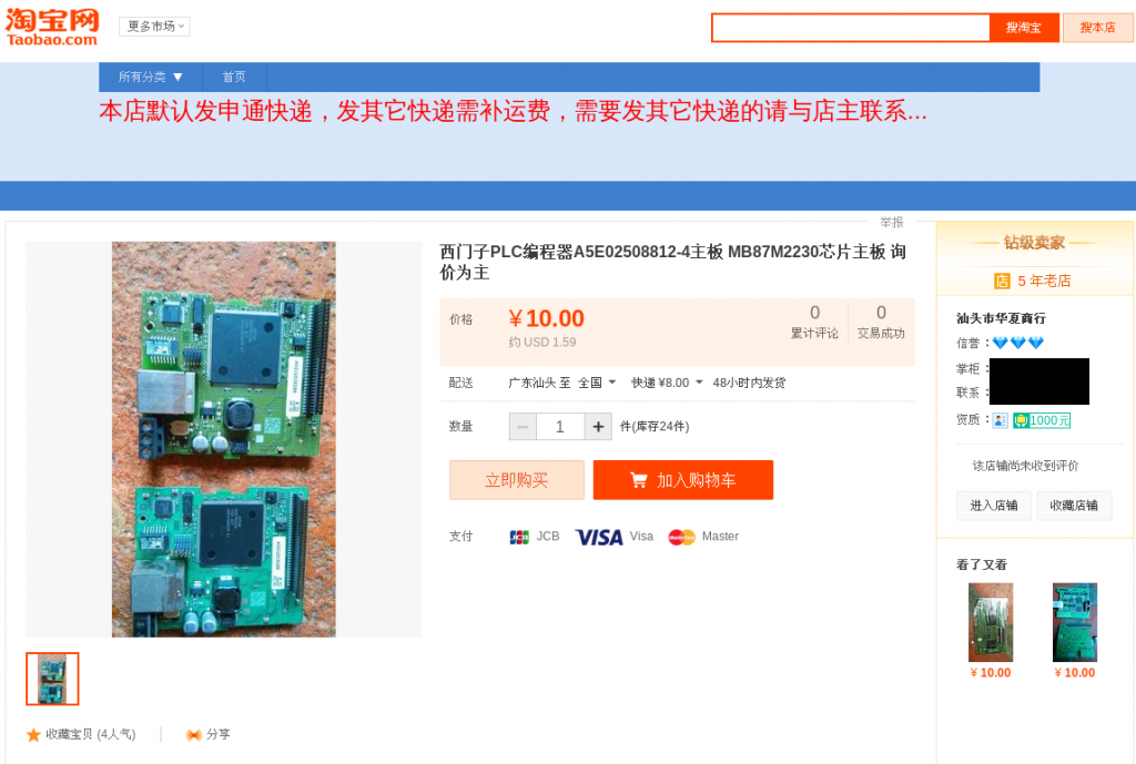
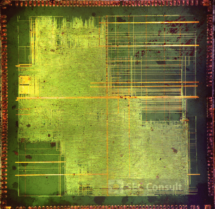
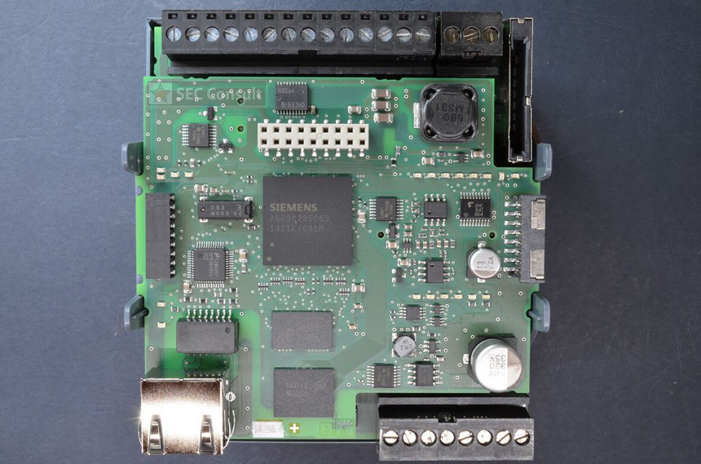
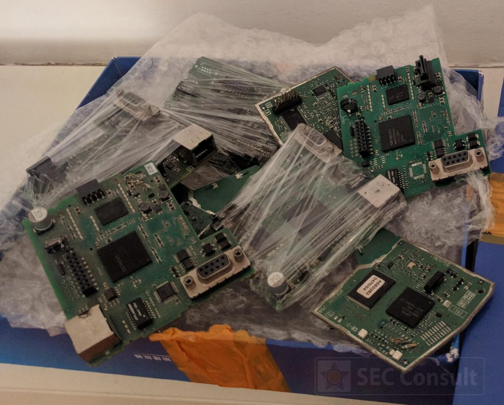
As ASICs are very specific solutions, it is not very likely that someone would manage to reverse engineer such a part without having access to scientific equipment like electron microscopes, wet-etching and so on. The fact that big vendors manufacture a lot of PCBs for their engineers and production, constitutes a potentially weak channel as information can be leaked. In some cases, these parts are even thrown away without further consideration or are sold to a local retailer. For these PLCs, PCBs with debug ports sometimes even end up in an online-shop on the Internet.

A week prior to the publication of this blogpost the following statement from Siemens reached us: The boards purchased by SEC Consult were not development boards but previously used or refurbished boards from Siemens devices. Siemens does not see a supply chain leak. Since the PLCs were apparently used in an older series of PLCs, our initial assumption of a supply-chain leak does not hold.

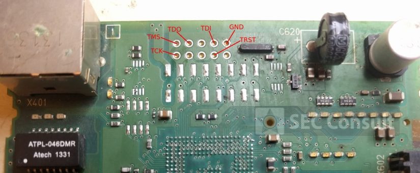
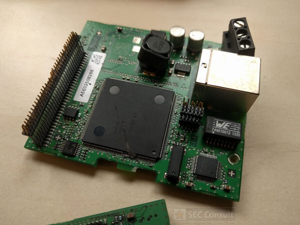
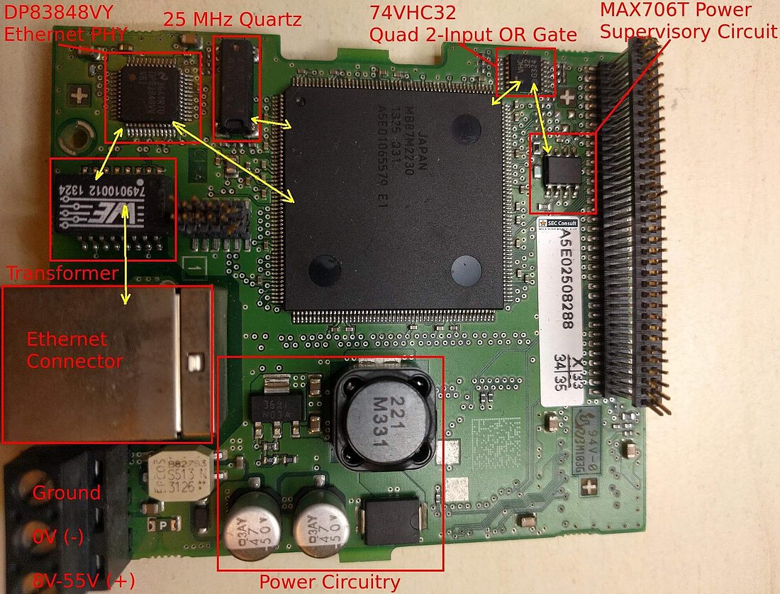
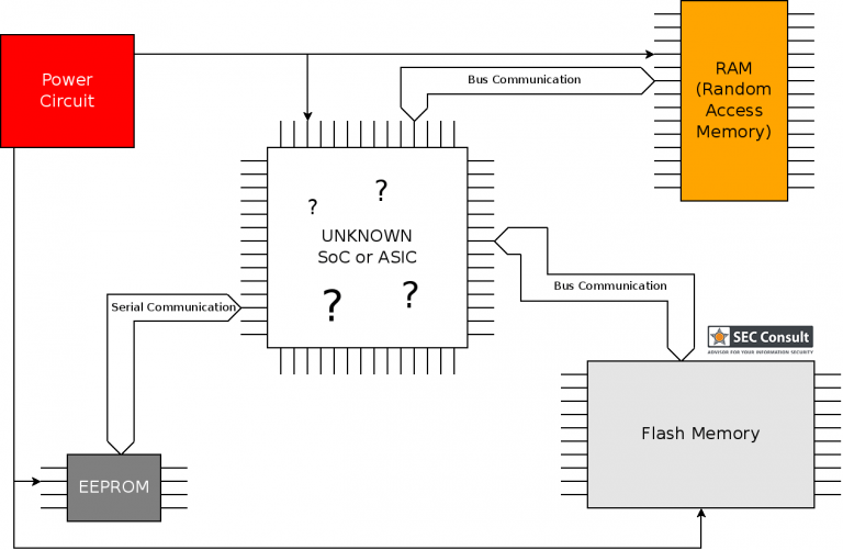
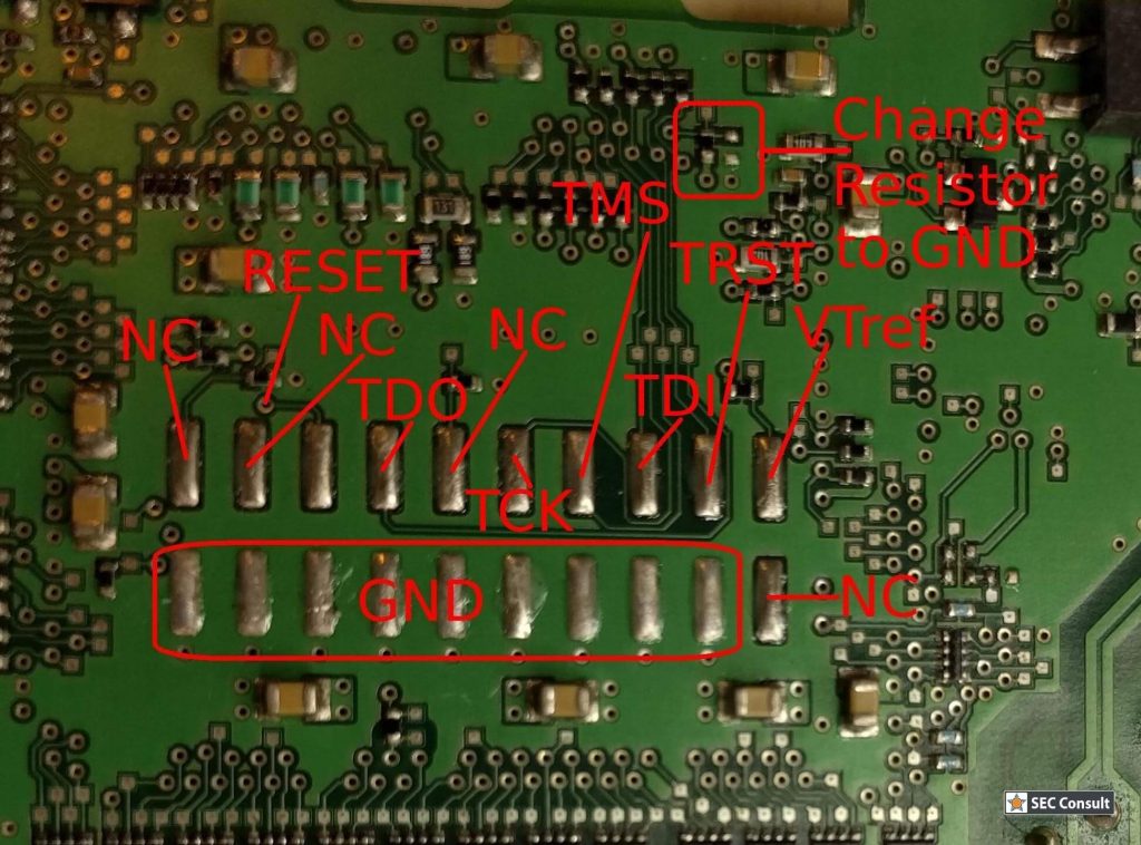
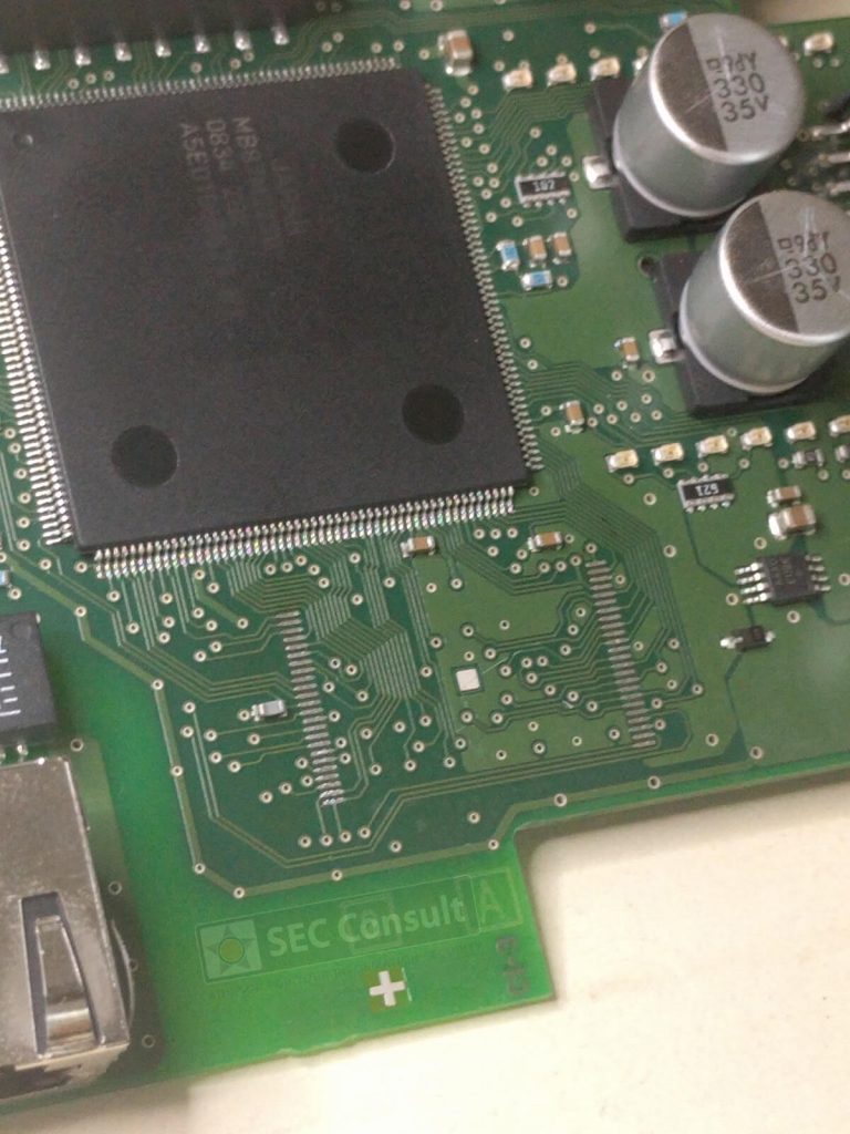
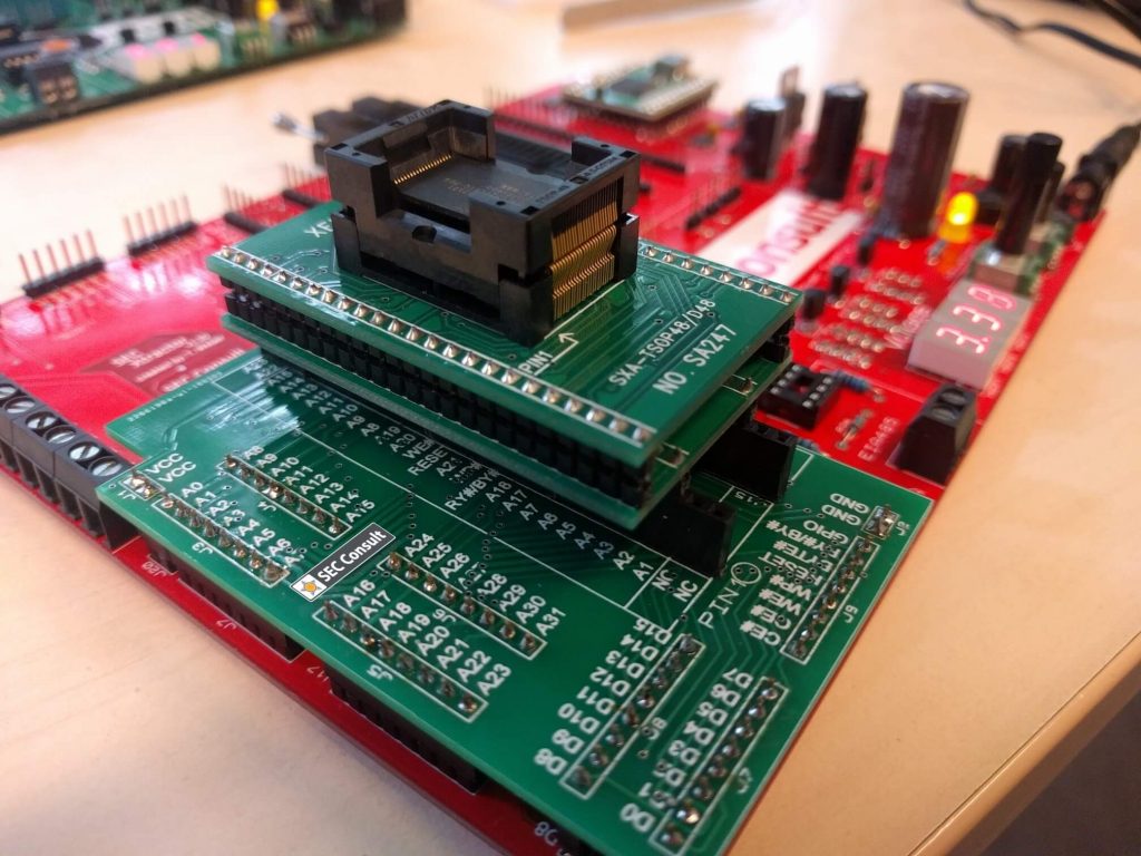
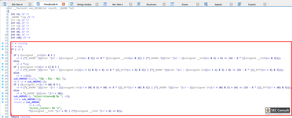
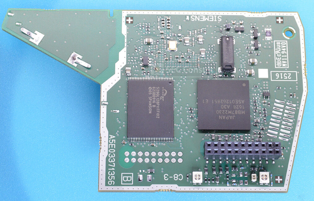
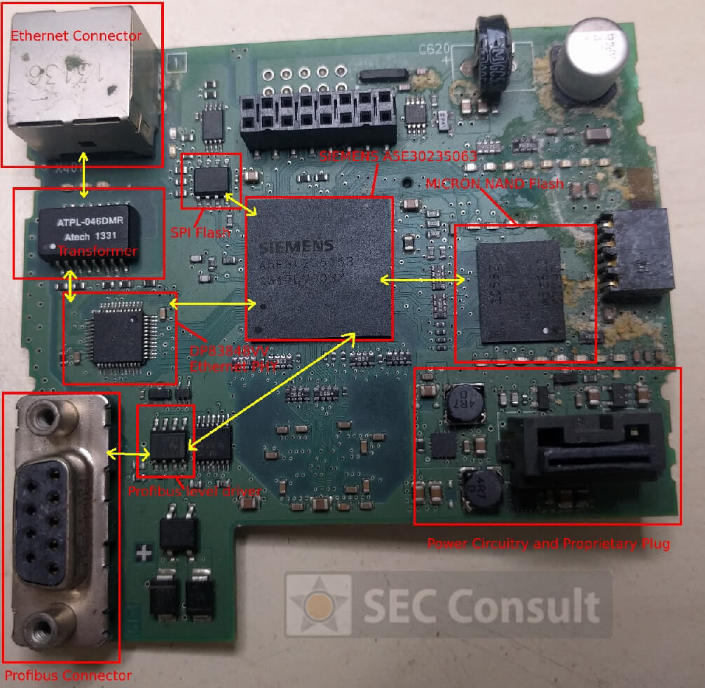
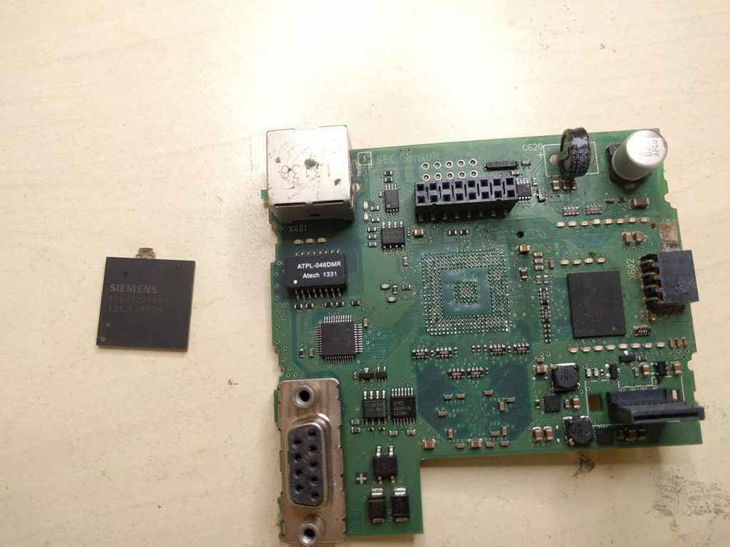
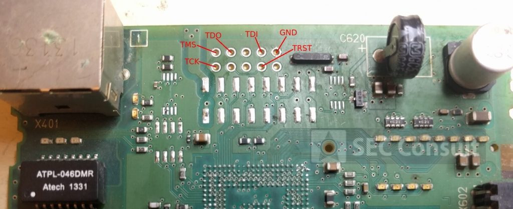
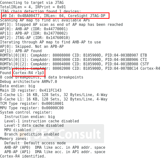
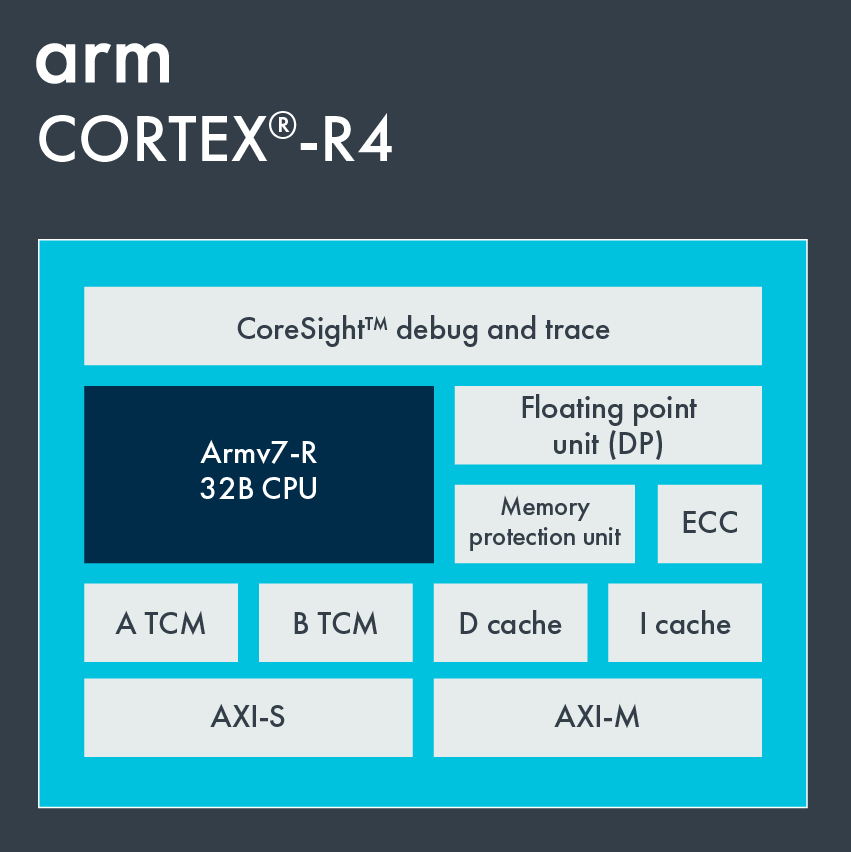
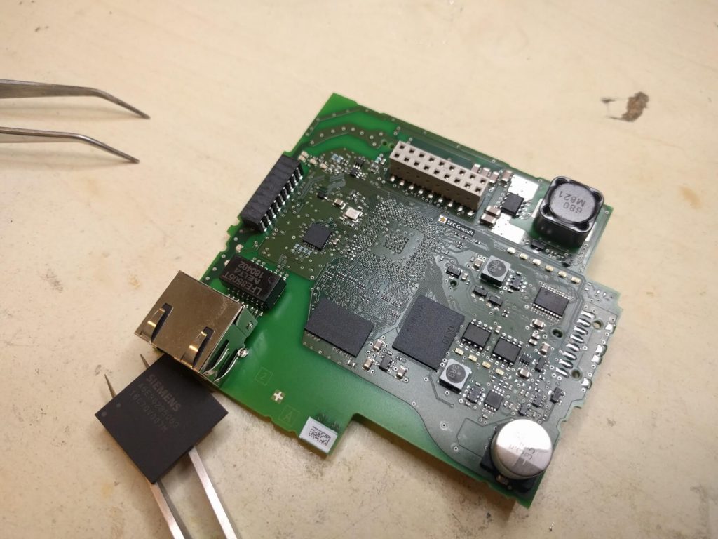
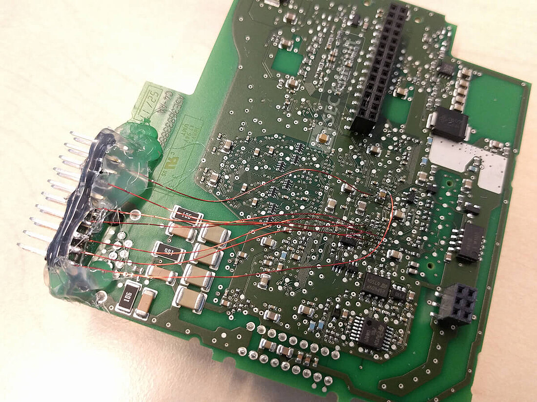
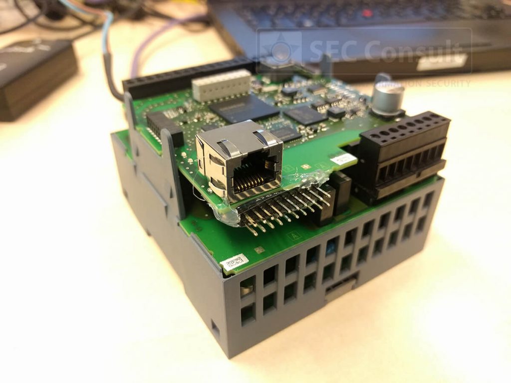
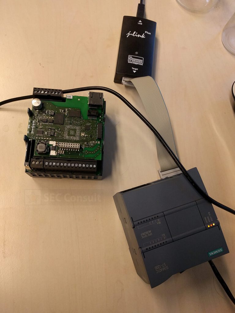
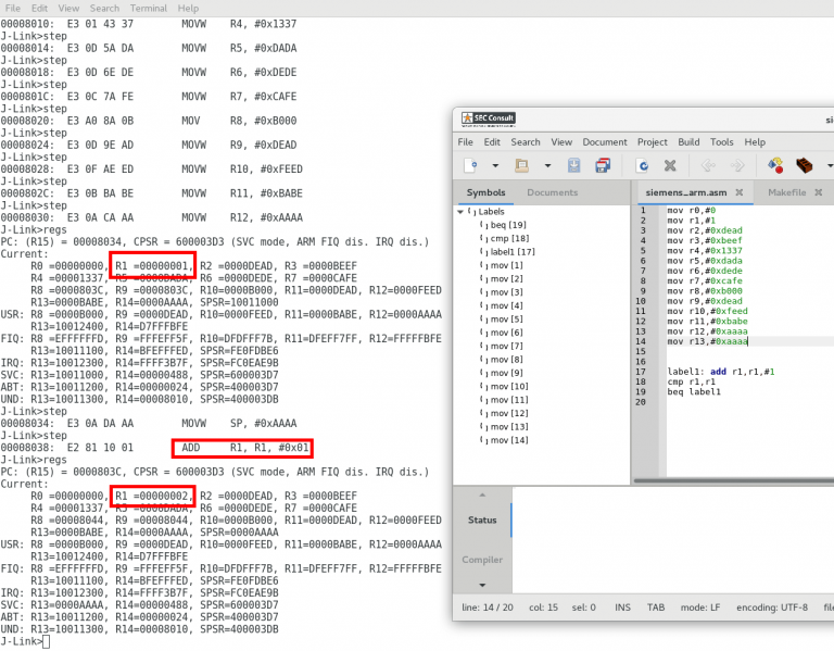
However, with few considerations and a structured approach it was indeed possible to reverse-engineer such boards. Finding out the debug-port of a custom chip was the first hurdle to overcome in order to debug and reprogram a chip. It became clear that one would gain full control over the device, in the end.

This means for the potential attackers:

  • Hardware backdoors could be installed on the PCB of the Siemens PLC.
  • All application programs on the PLC could be modified during run-time.
  • A PLC-persistent malware could be designed.
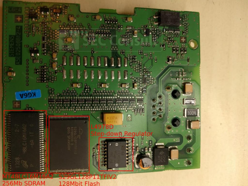
  • Since the NAND flash of the S7-1200v4 is write-able, it could be possible to place a backdoor in the firmware at this memory segment without leaving any trace (more complicated but invisible).

As attackers with such capabilities tend not to disclose such details, we assume that they might have known them for a while and there is the possibility that such PLCs could carry backdoors.

Better news for the security analysts:

  • A security researcher which has access to the pinout is able to search for firmware vulnerabilities on these devices.
  • Memory forensics, searching for backdoors, malware and other changes in the code of this PLC are possible too.
  • Hardware backdoors are more easily detectable as they will be connected to all of the pins which are used to debug the PLC.

In contrast to Bloomberg’s article “The Big Hack” which describes an IC of the size of an RF balun (RF conditioner), a general backdoor at that level will be hidden in firmware or a small hardware module (as big as a coin) at least. It is easier to hide such sophisticated chips in packages of other chips or even between the PCB layers instead of giving them a separate package.


This research was done by Thomas Weber on behalf of SEC Consult Vulnerability Lab